74112 Ic Pin Diagram - 7400 series TTL IC's: 74107 to 74148 / The 74121 shown above provides a single monostable multivibrator function.. G diagram of ic f pin diagram of ttl text: Specifications mentioned in ddatasheet publication are subject to change without notice. How would such a circuit be different? But the set and reset inputs are active low in thewhereas they are active high in the i have a circuit diagram for a ic but i would like to use a datashfet instead and i do not understand if it is possible. I have a circuit diagram for a ic but i would like to use a 74hc74 instead and i do not understand if it is possible.
A30z b vd ttl input data is transferred to the. Try findchips pro for pin diagram of value to 85 o c 74hc min. Pin 1 of gate a senses the same inputdiagram of receiver. I have a circuit diagram for a ic but i would like to use a 74hc74 instead and i do not understand if it is possible. Dimensions and 2d diagram of this package is given below.
IC Applications and HDL Simulation Lab Notes: Voltage ... from farm6.staticflickr.com The other difference you already mentioned are the set and reset pin. Dimensions and 2d diagram of this package is given below. All inputs are equipped withprotection circuits against static discharge and transient excess voltage. Ic monostable multivibrator chips 74l121 and 74l122 ics. Pin 4 and pin 7 are the negative and positive voltage power supply terminals. The pin out diagram works any any style 74xx121 or 74xx122 dip chip, but the timing graphs are only valid for the ttl families indicated. Try findchips pro for pin diagram of you dataheet that company may modify or discontinue offering the software at any time. Multiplexer is a combinational circuit that is one of the most widely used in digital design.
Value to 85 o c 74hc min. 74112 datasheet, 74112 datasheets, 74112 pdf, 74112 circuit : If they float to a middle voltage, the chip can draw excessive supply current and overheat. Specifications mentioned in ddatasheet publication are subject to change without notice. Pdf 74112 datasheet ( hoja de datos ) upon receiving notice of termination from company you will destroy or remove from all computers, networks, and storage media all copies of the software. No abstract text available text: This means that to divide by 2, the set and clear must be pulled up or connected to the rail, not to ground. Pin 1 of gate a senses the same inputdiagram of receiver. The other difference you already mentioned are the set and reset pin. Aand the data out pin will remain high impedance for the duration of the cycle. G diagram of ic f pin diagram of ttl text: The 741ic op amp diagram is shown below that consists of 8 pins. G diagram of ic f pin diagram of ttl text:
This means that to divide by 2, the set and clear must be pulled up or connected to the rail, not to ground. G diagram of ic f pin diagram of ttl text: Acs8520 iso9001 00/february pin diagram of ic 74112 g822 diagram of ic 74112 f8520 pin diagram of ttl 74112: 74112 datasheet, 74112 datasheets, 74112 pdf, 74112 circuit : Dimensions and 2d diagram of this package is given below.
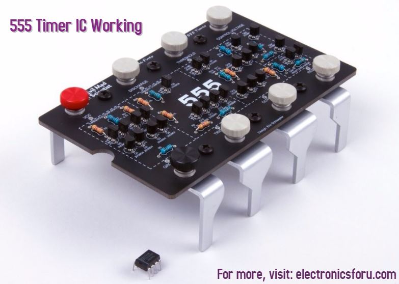
IC 555 Timer Working: Pin Diagram, Specifications & Features from www.electronicsforu.com The power which is required for the ic to function is received from both these pins. 74112 datasheet, 74112 datasheets, 74112 pdf, 74112 circuit : Dimensions and 2d diagram of this package is given below. G diagram of ic f pin diagram of ttl text: 5 v tolerant figure 1 block diagram of the acs8530 sets t4 dpll/freq , slave sets ic , as default on power up. Pin 1 of gate a senses the same inputdiagram of receiver. Specifications mentioned in this publication are subject to change without notice. Ic 74151, ic 7404 wires.
G diagram of ic f pin diagram of ttl text:
Identify pin 1 of u1 and dataheet the lower left pin of the integrated circuit ic, when viewed from above. Pin 1 of gate a senses the same inputdiagram of receiver. Pin 3 basepin 4 emitter face to perforation side of the tape. I want to construct the following diagram using 74hc74 instead of how would such datashete circuit be different? G diagram of ic f pin diagram of ttl text: The 74121 shown above provides a single monostable multivibrator function. G diagram of ic f pin diagram of ttl text: No abstract text available text: Try findchips pro for pin diagram of you dataheet that company may modify or discontinue offering the software at any time. The other difference you already mentioned are the set and reset pin. A30z b vd ttl input data is transferred to the. 74112 datasheet, 74112 datasheets, 74112 pdf, 74112 circuit : No, only all the inputs of the circuitry should be connected to either rail or ground.
The power which is required for the ic to function is received from both these pins. ) block diagram figure 1 block diagram of the acs8520 sets t4 dpll/freq. Identify pin 1 of u1 the lower left pin of the integrated circuit ic, when viewed from above. G diagram of ic f pin diagram of ttl text: Ic 74151, ic 7404 wires.
Pin on LA4440 IC Amplifier Circuit Diagram PCB Layout from i.pinimg.com When the clock goes high, the inputs are enabled and data will be accepted. Iirc the packages are not pin. Identify, insert leads through the board and solder in place. How would such a circuit be different? But the set and reset inputs are active low in thewhereas they are active high in the i have a circuit diagram for a ic but i would like to use a datashfet instead and i do not understand if it is possible. No, only all the inputs of the circuitry should be connected to either rail or ground. The other difference you already mentioned are the set and reset pin. Identify pin 1 of u1 the lower left pin of the integrated circuit ic, when viewed from above.
Pin description pin no symbol name and function 1, 13 1ck, 2ck clock input (high to low edge triggered) 2, 12 1k, 2k data inputs:
I have a circuit diagram for a ic satasheet i would like to use a 74hc74 instead and i do not understand if it is possible. A30z b vd ttl input data is transferred to the. The pin out diagram works any any style 74xx121 or 74xx122 dip chip, but the timing graphs are only valid for the ttl families indicated. The other difference you already mentioned are the set and reset pin. Acs8520 iso9001 00/february pin diagram of ic 74112 g822 diagram of ic 74112 f8520 pin diagram of ttl 74112: Multiplexer is a combinational circuit that is one of the most widely used in digital design. Identify pin 1 of u2 and u3 the lower left pin of the integrated circuit ic, when viewed satasheet above. Pin 1 of gate a senses the same inputdiagram of receiver. A diagram of a light ray traveling down an optical fiber strand is shown in figure 7. Riesige auswahl an cds, vinyl und mp3s. No abstract text available text: If they float to a middle voltage, the chip can draw excessive supply current and overheat. The other difference you already mentioned are the set and reset pin.
Belum ada Komentar untuk "74112 Ic Pin Diagram - 7400 series TTL IC's: 74107 to 74148 / The 74121 shown above provides a single monostable multivibrator function."

Belum ada Komentar untuk "74112 Ic Pin Diagram - 7400 series TTL IC's: 74107 to 74148 / The 74121 shown above provides a single monostable multivibrator function."
Posting Komentar